Chemical Vapour Deposition System
Chemical Vapour
Deposition System
Chemical Vapour Deposition System
Chemical Vapor Deposition (CVD) is a high-temperature process used to deposit thin films by chemically reacting vapor-phase precursors on heated substrates. These systems are essential for producing semiconductors, nanomaterials, optoelectronics, and protective coatings.
Our portfolio of CVD systems includes both Hot Wall and Cold Wall configurations each designed with precision, flexibility, and process control in mind. With over 50 custom-developed systems, we cater to a broad spectrum of research and industrial requirements.
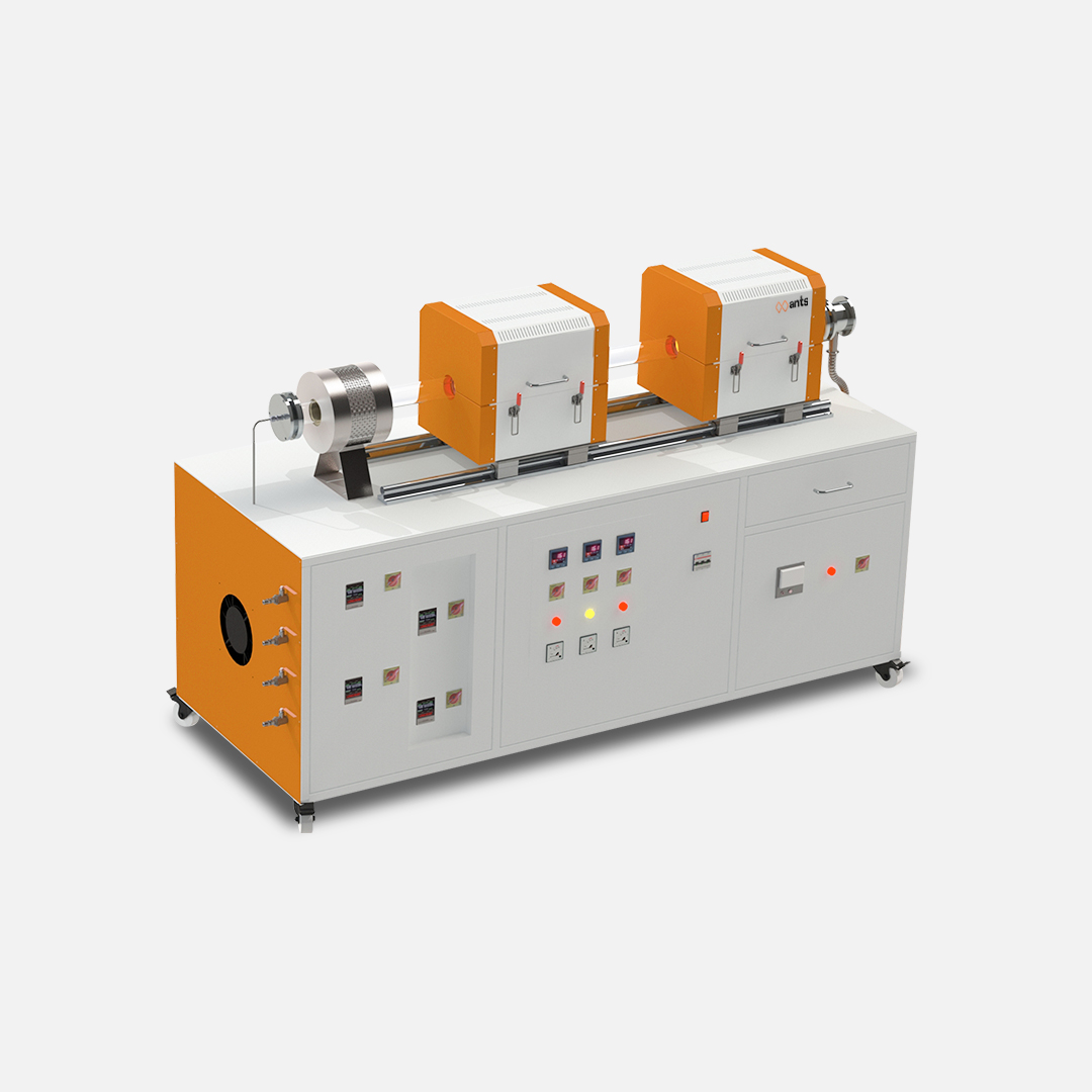
Hot Wall
CVD Systems
Hot Wall CVD Systems
Uniform chamber heating ensures consistent deposition, making them ideal for applications like photovoltaic coatings, refractory ceramics, and optical layers. We offer reaction tube diameters up to 120 mm and multi-zone heating for superior process control.
Applications:
- Dielectric layers for semiconductors
- Ceramic & wear-resistant coatings
- Solar cell manufacturing
Cold Wall
CVD Systems
Cold Wall CVD Systems
Only the substrate is heated, keeping chamber walls cool to prevent unwanted deposition. This enables faster cycling, high purity, and is ideal for sensitive nanomaterials.
Applications:
- Graphene & carbon nanotube synthesis
- MEMS & microelectronics
- Barrier & conductive films for packaging
Customized CVD Configurations & Capabilities
Our CVD systems are designed with flexibility and performance in mind supporting a range of process types, control options, and heating architectures to meet diverse application needs.
Heating Architecture
Inductive heating for highly uniform substrate temperature
Multi-zone control for consistent thermal gradients
Heating Architecture
Inductive heating for highly uniform substrate temperature
Multi-zone control for consistent thermal gradients
Atmosphere Control
Vacuum, inert, or reducing environments
Precise gas flow management using multi-channel MFCs
Atmosphere Control
Vacuum, inert, or reducing environments
Precise gas flow management using multi-channel MFCs
Automation & Interface
Fully automated systems with digital touchscreen interfaces
Customizable process recipes and safety interlocks
Automation & Interface
Fully automated systems with digital touchscreen interfaces
Customizable process recipes and safety interlocks
Available Process Types
APCVD
Atmospheric Pressure CVD:
Ideal for industrial coatings & solar
cells
LPCVD
Low Pressure CVD:
Ensures uniform thin films for
semiconductors
MOCVD
Metal Organic CVD:
For LEDs, laser diodes, and
optoelectronic materials
- Temperature Range: Up to 1600°C
- Gas Flow: Multi-channel MFCs for accurate delivery
- Reactor Options: Single or multi-zone tube setups
- Control Interface: Digital touchscreen with recipe programming
- Safety Systems: Over-temperature alarms, leak detection, emergency shut-off
- Semiconductor Fabrication
- Nanomaterials & Graphene Synthesis
- Advanced Coatings
- Photovoltaic Cell Production
- Biomedical Coatings
- Optoelectronics