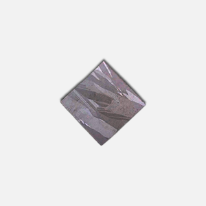
Silicon Substrate - Silicon Wafer
Price Range
₹854.00
Processing Time : 7 To 10 Business Days
Ships from Mumbai Warehouse
Country of Origin: India
Solar Multicrystalline Silicon Substrate /Silicon Wafer
Furthermore, Silicon wafers are one of an essential component in almost every modern electronic or consumer item. The contemporary society uses it in varied forms for numerous applications. Certainly, silicon is the 2nd most common element on earth is a common semiconductor. Likewise, There are various methods for processing silicon into wafers. The most popular ones include the Czochralski (Cz) pulling method and the Float Zone (FZ) growth method.
Silicon wafer uses the famous Cz method. Aforementioned involves pulling a ‘seed’ crystal from the melting process. A pure crystalline silicon cylinder grew in this way. Once the entire cylinder formed from the single silicon crystal, the wafers are extracted using the ‘wire-cutting’ technique. Very tiny and thin slices of crystalline silicon sliced from the cylinder. Therefore silicon wafers are used worldwide for the production of microchips, semiconductors, and transistors. Above all Silicon is a hard and brittle material.
TYPES OF SILICON WAFER
There are two types of varieties available in silicon wafer such as doped and un-doped. A un-doped type is a pure form of silicon, whereas the doped is non-pure form in which a few elements have added in the form of impurities or dopant. The un-doped is known as intrinsic silicon wafer while the doped termed as extrinsic or degenerate wafer depends on the amount of doping. If a doping amount is tiny/moderate, then it is the extrinsic type and on another hand, if doping quantity is high, then it is Degenerate type. The doping is necessary to change the electrical property of the material. In research and industry, doped one used extensively. There are two doped substrate one is a positive i.e. P-type silicon wafer, and another is negative (N-type) silicon wafer. Generally, during the process of silicon fabrication the boron added to produce P-type material and Phosphorus, Antimony, Arsenic doped to make N-type material. In this, the N-type wafer has some negatively charged electrons while P-type has some number of positively charged holes.Finally, the following are the applications of silicon wafers
- Manufacturing of semiconductors
- Laptops and Desktop computers
- Mobile smartphones, tablet-phones, and other wearable smart gadgets Home appliances
- Microchips
- Thin-film deposition process
- Calibrating instruments
- R&D and manufacturing
- Automobiles, aerospace and drone technology
- AI (Artificial Intelligence)
- MEMS fabrication
- Transistors, diodes, and rectifiers
- Robotics
- Solar cell
- ICs (Integrated Circuits)
- High-power applications (detectors and sensor devices)
- Opto-Electronic components
| General Characteristics | Features |
| Growth Method | Directional |
| Conductivity Type | P-Type |
| Dopant | Boron |
| Resistivity | 0.5-2 Ω cm |
| Oxygen Content | 8 × 10¹⁷ atom/ cm3 |
| Carbon Content | 5 × 10¹⁶ atom/ cm3 |
| Structural Characteristics | Features |
| Side | 156mm +/- 0.5 mm |
| Corner Diagonal | 1.5mm +/- 0.5mm |
| Corner Angle | 900 +/- 0.30 |
| Thickness | 200 +/-20pm |
| Surface | Unpolished |
| Mechanical Characteristics | Features |
| TTV | <= 50 µm |
| Bow | <= 60 µm |
| Saw Mark | <= 15 µm |
Add a Review
There are no reviews yet. Be the first to review "Silicon Substrate - Silicon Wafer" Your email address will not be published. Required fields are markedYour rating
Your review
This field is required.Name
This field is required.Something went wrong, we could not submit review.


